


PCB (Printed Circuit Board) is a conducive pattern applied on one both sides of a substrate where electronic components are soldered to complete a circuit. We will be preparing and making our Printed Circuit Board using Copper Clad Board as shown above. Actually it is done when we already have our circuit design on the bondpaper.
Steps for CCB PCB Preparation/Making
1.) Cut copper clad board to specified size (e.g. 5"x 5"). The size is dependent on the number and sizes of electronic components present in a circuit design.
2.) Straighten or smoothen the edges by filing or by sandpaper. This is to avoid sharp or pointed corners and edges which would be the cause of wounds.
3.) If you have seen unnecessary marks on the copperside (e.g. pen marks, pencil marks, dirt), clean using an eraser. DO NOT USE sandpaper in erasing the unnecessary marks.
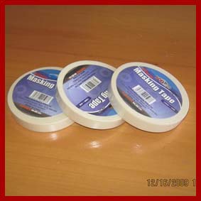
4.) Cover copperside with masking tape. It would be necessary if the masking tape has greater width. Be sure the tape is firmly in contact with the copper. This to avoid for the "wanted" copper to be removed by the Ferric chloride when etched.

5.) Photocopy your PCB Layout. After you made your PCB layout on a bondpaper, you need to have it photocopied to have an extra just in case you got mistake in cutting your PCB design on the board.
6.) Cut and glue the photocopied PCB Layout on top of masking tape.
7.) Wait for few minutes until it dries.
8.) Punch the holes (circular in shapes) using prick punch and a hammer. Avoid using too much force as this well break your board and will ruin your design.
10.) Peel-off the cut-out unwanted layout exposing the copper. Do not do this as if you are in a hurry because there will possibilities you haven't cut your layout properly that will result for the exposure of wanted copper.

11.) Etch your Copper Clad Board using the Ferric Chloride solution.
12.) When you are done etching your design, rinse the board with flowing water.
13.) Remove the masking tape.
14.) Drill the holes using a mini drill
15.) Solder your electronic components.
Soldering is a broad topic. I will impart my ideas about soldering in my next post. Actually PCB Preparation/Making using Presensitized board is quite similar to Copper Clad Board but neglecting some of its steps, because in this process, you will not be using cutter and masking tape anymore. Aside from that your circuit design will be in a tracing paper and you will be using the sunlight or the Ultraviolet rays for transferring the circuit design to your board. I will talk more on these in a post next time.

Nice Salcedo | On: June 2, 2010 at 5:16 AM
hmm..this is a useful tutorial.. :D thanks for sharing! :)
Jhiegzh | On: June 2, 2010 at 5:41 AM
@Nice: Karelate ka? ^^
Sasarai | On: June 2, 2010 at 7:36 AM
Aba aba Jigs ha! Yan pala ang naidudulot ng may "engineering" sa course natin! Muahahaha! Sad to say., ndi namin nagawa yang etching... may circuit nga, wala namang board. sayang lang. T_T Tsaka Universal PCB gamit namin nun, (yung may mga etches na sa likod tas butas meron na rin, just plug every components...) I just don't like what our Computer Workshop did to us.... He didn't even taught those! Wew. Natutunan ko lang kung paano magsolder sa makakapal na copper wires forming a cube. Nakakaasar lang. pero good tutorial! Minsan magtatry kong magetch ng isang circuit, but not now! OK :))
JHEN | On: June 2, 2010 at 7:49 AM
ako. hindi ako nakarelate. hehe. pero. that's very a nice and helpful tut ^^
Life Moto | On: June 2, 2010 at 10:53 AM
informative bro lalo na sa field ng electronics. I suggest create ka ng tech blog too.
Jhiegzh | On: June 2, 2010 at 5:27 PM
@Juls: Ah okay universal pla! Madali n pla sa inyo gumawa ng output kung ganun! Sure you can!
@Jhen: Thanks, hahah!
@LifeMoto: Uhmm, next time, can't handle 2 blogs same time..^^
aryan | On: June 2, 2010 at 9:11 PM
shucks, nose bleed. haha. but it's a good thing you posted that, i think were doing that this year for my course. salamat Jhiegzh.
Jhiegzh | On: June 2, 2010 at 9:58 PM
@Aryan: Applicable lang yan kung gamitin mo Copper Clad Board, iba rin ung steps kung Presensitized! ^^ Thanks for appreciation!
Superjaid | On: June 2, 2010 at 10:35 PM
nose bleed!waahhh..hehehe
Nikki | On: June 2, 2010 at 11:03 PM
cool :) thanks for the tut kuya :D ang hirap aa.
Sasarai | On: June 3, 2010 at 12:44 AM
Hindi rin Jigs, kasi kailangan mo pang itrace ng itrace ... and probably bawal na yun for future projects... :)) Kaya ayun, I also need this, pero meron na rin kasi ito sa workbook ko sa workshop. ^_^
Jhiegzh | On: June 3, 2010 at 3:37 AM
@Superjaid: Bkit naman nosebleed?
@Cheen: D naman!
@Juls: Ah awkie ^^
sasha | On: June 4, 2010 at 4:13 AM
nice blog la...........
Jhiegzh | On: June 4, 2010 at 5:17 AM
@Sasha" Thank you!
Anonymous | On: January 26, 2011 at 6:48 AM
saan yung tutorial nya??